- 您现在的位置:买卖IC网 > Sheet目录3831 > PIC18F2515-I/SO (Microchip Technology)IC MCU FLASH 24KX16 28SOIC
PIC18F2X1X/4X1X
DS39636D-page 144
2009 Microchip Technology Inc.
15.4.4
HALF-BRIDGE MODE
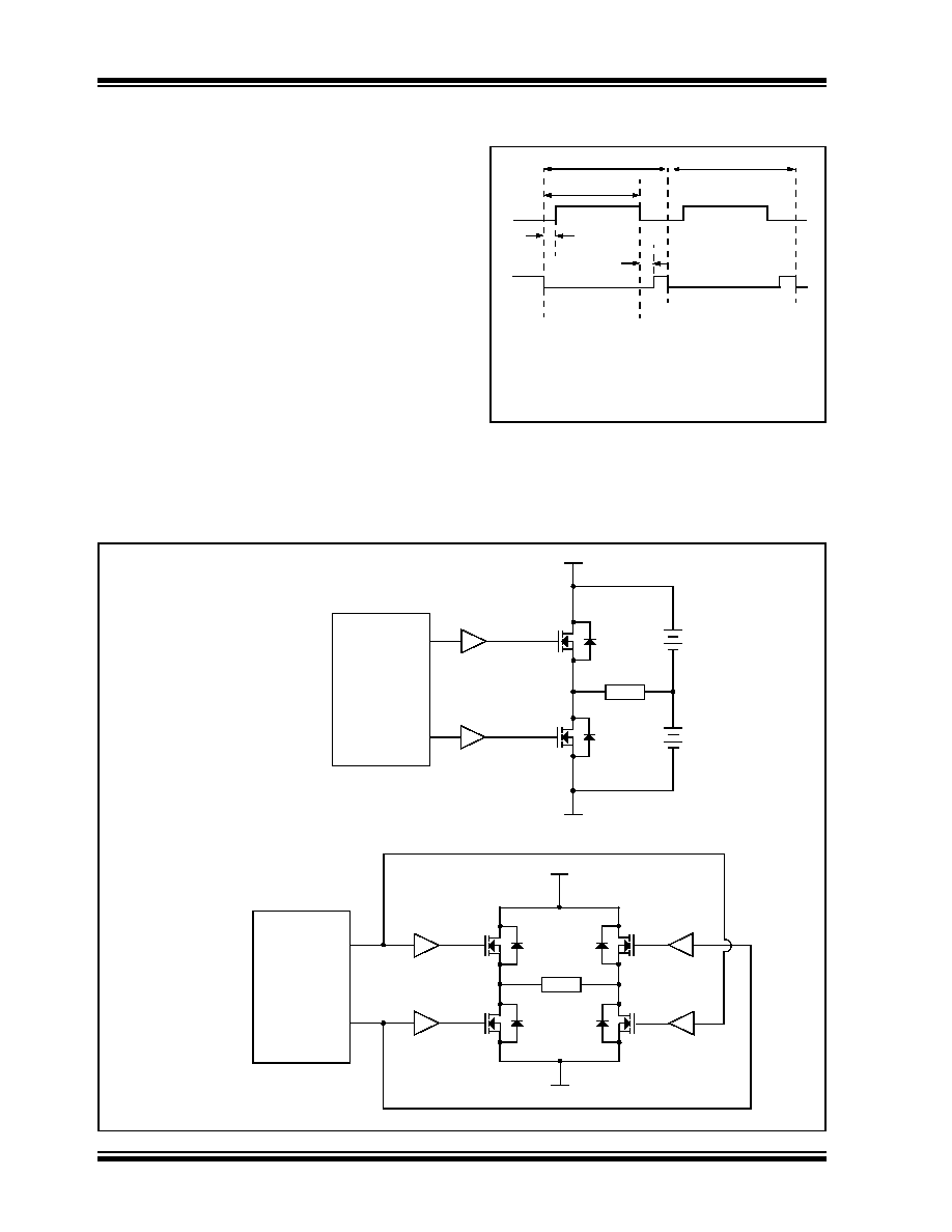
In the Half-Bridge Output mode, two pins are used as
outputs to drive push-pull loads. The PWM output
signal is output on the P1A pin, while the complemen-
tary PWM output signal is output on the P1B pin
(Figure 15-4). This mode can be used for half-bridge
applications, as shown in Figure 15-5, or for full-bridge
applications where four power switches are being
modulated with two PWM signals.
In Half-Bridge Output mode, the programmable dead-
band delay can be used to prevent shoot-through
current in half-bridge power devices. The value of bits
PDC6:PDC0 sets the number of instruction cycles
before the output is driven active. If the value is greater
than the duty cycle, the corresponding output remains
inactive during the entire cycle. See Section 15.4.6
“Programmable Dead-Band Delay” for more details
of the dead-band delay operations.
Since the P1A and P1B outputs are multiplexed with
the PORTC<2> and PORTD<5> data latches, the
TRISC<2> and TRISD<5> bits must be cleared to
configure P1A and P1B as outputs.
FIGURE 15-4:
HALF-BRIDGE PWM
OUTPUT
FIGURE 15-5:
EXAMPLES OF HALF-BRIDGE OUTPUT MODE APPLICATIONS
Period
Duty Cycle
td
(1)
P1A(2)
P1B(2)
td = Dead-Band Delay
Period
(1)
Note 1: At this time, the TMR2 register is equal to the
PR2 register.
2: Output signals are shown as active-high.
PIC18F4X1X
P1A
P1B
FET
Driver
FET
Driver
V+
V-
Load
+
V
-
+
V
-
FET
Driver
FET
Driver
V+
V-
Load
FET
Driver
FET
Driver
PIC18F4X1X
P1A
P1B
Standard Half-Bridge Circuit (“Push-Pull”)
Half-Bridge Output Driving a Full-Bridge Circuit
发布紧急采购,3分钟左右您将得到回复。
相关PDF资料
DSPIC33FJ128GP202-I/SP
IC DSPIC MCU/DSP 128K 28DIP
PIC24FJ128GA310-I/BG
MCU 16BIT 128KB FLASH 121TFBGA
PIC24HJ128GP204-I/PT
IC PIC MCU FLASH 128K 44TQFP
PIC18F8393-I/PT
IC PIC MCU FLASH 4KX16 80TQFP
DSPIC33FJ128GP204-I/PT
IC DSPIC MCU/DSP 128K 44TQFP
DSPIC33FJ64MC802-I/MM
IC DSPIC MCU/DSP 64K 28-QFN
PIC16F876A-I/SS
IC MCU FLASH 8KX14 EE 28SSOP
PIC24HJ128GP202-I/SP
IC PIC MCU FLASH 128K 28DIP
相关代理商/技术参数
PIC18F2515-I/SP
功能描述:8位微控制器 -MCU 48KB 3968 RAM 25 I/O RoHS:否 制造商:Silicon Labs 核心:8051 处理器系列:C8051F39x 数据总线宽度:8 bit 最大时钟频率:50 MHz 程序存储器大小:16 KB 数据 RAM 大小:1 KB 片上 ADC:Yes 工作电源电压:1.8 V to 3.6 V 工作温度范围:- 40 C to + 105 C 封装 / 箱体:QFN-20 安装风格:SMD/SMT
PIC18F2515T-I/SO
功能描述:8位微控制器 -MCU 48KB 3968 RAM 25 I/O RoHS:否 制造商:Silicon Labs 核心:8051 处理器系列:C8051F39x 数据总线宽度:8 bit 最大时钟频率:50 MHz 程序存储器大小:16 KB 数据 RAM 大小:1 KB 片上 ADC:Yes 工作电源电压:1.8 V to 3.6 V 工作温度范围:- 40 C to + 105 C 封装 / 箱体:QFN-20 安装风格:SMD/SMT
PIC18F2520-E/ML
功能描述:8位微控制器 -MCU 32KB 3968 RAM 25I/O RoHS:否 制造商:Silicon Labs 核心:8051 处理器系列:C8051F39x 数据总线宽度:8 bit 最大时钟频率:50 MHz 程序存储器大小:16 KB 数据 RAM 大小:1 KB 片上 ADC:Yes 工作电源电压:1.8 V to 3.6 V 工作温度范围:- 40 C to + 105 C 封装 / 箱体:QFN-20 安装风格:SMD/SMT
PIC18F2520-E/SO
功能描述:8位微控制器 -MCU 32KB 3968 RAM 25I/O RoHS:否 制造商:Silicon Labs 核心:8051 处理器系列:C8051F39x 数据总线宽度:8 bit 最大时钟频率:50 MHz 程序存储器大小:16 KB 数据 RAM 大小:1 KB 片上 ADC:Yes 工作电源电压:1.8 V to 3.6 V 工作温度范围:- 40 C to + 105 C 封装 / 箱体:QFN-20 安装风格:SMD/SMT
PIC18F2520-E/SP
功能描述:8位微控制器 -MCU 32KB 3968 RAM 25I/O RoHS:否 制造商:Silicon Labs 核心:8051 处理器系列:C8051F39x 数据总线宽度:8 bit 最大时钟频率:50 MHz 程序存储器大小:16 KB 数据 RAM 大小:1 KB 片上 ADC:Yes 工作电源电压:1.8 V to 3.6 V 工作温度范围:- 40 C to + 105 C 封装 / 箱体:QFN-20 安装风格:SMD/SMT
PIC18F2520-I/ML
功能描述:8位微控制器 -MCU 32kBF 1536RM 25I/O RoHS:否 制造商:Silicon Labs 核心:8051 处理器系列:C8051F39x 数据总线宽度:8 bit 最大时钟频率:50 MHz 程序存储器大小:16 KB 数据 RAM 大小:1 KB 片上 ADC:Yes 工作电源电压:1.8 V to 3.6 V 工作温度范围:- 40 C to + 105 C 封装 / 箱体:QFN-20 安装风格:SMD/SMT
PIC18F2520-I/ML
制造商:Microchip Technology Inc 功能描述:8-Bit Microcontroller IC
PIC18F2520-I/SO
功能描述:8位微控制器 -MCU 32KB 1536 RAM 25I/0 RoHS:否 制造商:Silicon Labs 核心:8051 处理器系列:C8051F39x 数据总线宽度:8 bit 最大时钟频率:50 MHz 程序存储器大小:16 KB 数据 RAM 大小:1 KB 片上 ADC:Yes 工作电源电压:1.8 V to 3.6 V 工作温度范围:- 40 C to + 105 C 封装 / 箱体:QFN-20 安装风格:SMD/SMT